
Nvidia N1X (48SM): Specs of a Shared-Memory Blackwell Laptop GPU, and Where Sources Disagree
A 6144-shader Blackwell chip sharing up to 128 GB of memory with a 20-core Grace CPU looks strong on paper, but clocks, cache, node and DLSS version vary by source.
Contents
- Nvidia N1X (48SM) at a glance: an integrated Blackwell laptop GPU released June 1, 2026
- 6144 shaders, 48 compute units and 24 MB of shared cache: the core layout
- Ray-tracing hardware: 48 fourth-generation RT cores and RTX support
- Clock speeds and raw performance: 1665/2535 MHz and 31.2 FP32 TFLOPS on the spec sheet
- Shared memory: up to 128 GB on a 256-bit bus, with no dedicated VRAM
- Can the N1X (48SM) run large AI models locally?
- The 20-core Grace pairing and what the N1X name means
- AI performance and power: 1 petaflop and a 45 to 80 W envelope
- Supported graphics and compute APIs: versions at a glance
- DLSS support: DLSS 4 on the spec, DLSS 5 on NVIDIA's table
- Interface and connectors: PCI Express Gen 5, one HDMI output and no extra power connector
- Manufacturing: a 3 nm node and 173.6 mm² die on the spec, 5 nm on Technical City
- Windows 11, Studio and Game Ready drivers, and NVIDIA software features
- Where it sits: a mid-range label, an Apple M5 Max comparison and no top-100 ranking
- Who the N1X (48SM) suits, and who should look elsewhere
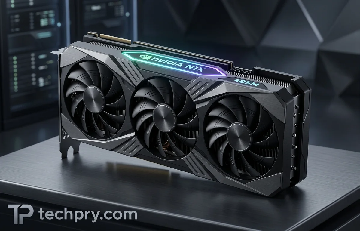
The N1X (48SM) is the graphics half of a laptop chip, not a card you can add or swap: a 6144-shader Blackwell GPU that draws on a memory pool of up to 128 GB shared with a 20-core Grace CPU. The harder part for anyone comparing laptops is that the published numbers do not all agree. Technical City differs from the spec on seven values, from base clock to manufacturing node, and NVIDIA's own table names a different DLSS version than the spec does. Shader counts, memory and API support hold steady wherever they are listed; clocks, texture units, cache and the process node are the entries to treat with care.
Nvidia N1X (48SM) at a glance: an integrated Blackwell laptop GPU released June 1, 2026
Nvidia is the vendor, and the part is an for laptops rather than a discrete card. It was released on June 1, 2026, a date the spec and Technical City both give. The listed architecture is Blackwell (N1x); the label also appears in NVIDIA's table and in shattered.io's description, while Technical City files the part under Blackwell 2.0. The codename is GB20B in both the spec and Technical City.
Two labels in the spec sit in tension. The stated purpose is professional, yet the market segment is mid-range. That combination frames it as a mid-tier laptop part aimed at professional work, so memory, AI features and driver support matter here as much as shader count.
6144 shaders, 48 compute units and 24 MB of shared cache: the core layout
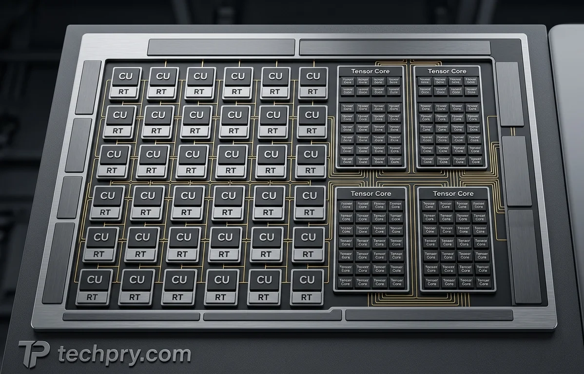
The GPU carries 6144 shading units, marketed as , alongside 192 texture mapping units, 48 render output units, 48 compute units, 192 and 48 ray-tracing cores. The spec adds 128KB of L1 cache per cluster and a 24MB shared .
| Block | Spec value | Do other sources agree? |
|---|---|---|
| Shading units | 6144 | Yes: shattered.io, NVIDIA's table and Technical City |
| Texture mapping units | 192 | No: Technical City lists 384 |
| Render output units | 48 | Yes: Technical City |
| Compute units | 48 | Spec only |
| Tensor cores | 192 | Yes: Technical City |
| Ray-tracing cores | 48 | Yes: Technical City |
| L1 cache | 128KB per cluster | Technical City lists 6 Mb |
| L2 cache | 24MB shared | No: Technical City lists 50 Mb |
Four of those rows are settled as far as the published figures go: the shader count is the same wherever it is listed, and Technical City matches the spec on ROPs, tensor cores and RT cores. The splits are the texture units and the L2. The TMU gap matters more than it looks, because texture fill rate follows from TMU count and clock, so the next section shows one disagreement running through several of Technical City's other numbers.
Cache figures are the hardest to compare. The spec's 24MB is a shared L2, whereas Technical City's 50 Mb carries a different unit label and no 'shared' qualifier, and its 6 Mb for L1 does not say per cluster, so the two lists cannot be lined up row by row.
For video work, NVIDIA's table lists one ninth-generation encoder and one sixth-generation decoder. Anyone planning heavy multi-stream encoding should check that a single engine of each type is enough.
Ray-tracing hardware: 48 fourth-generation RT cores and RTX support
Yes, the GPU handles in hardware: it has 48 RT cores of the fourth generation, and NVIDIA RTX is listed as supported. The spec and Technical City agree on the count of 48; the generation comes from NVIDIA's table alone.
Because the count equals the number of compute units, the layout suggests one RT core per compute unit, so ray-tracing capacity scales one-for-one with the compute block. These are capability figures, not frame rates, and they say nothing about how any particular game runs with ray tracing switched on.
Clock speeds and raw performance: 1665/2535 MHz and 31.2 FP32 TFLOPS on the spec sheet
On the spec sheet the base clock is 1665 MHz and the is 2535 MHz, with 2 instructions per cycle feeding a pixel fill rate of 122 GPixel/s, a texture fill rate of 487 GTexel/s and 31.2 TFLOPS of . Technical City lists 741 MHz base, 2346 MHz boost, a texture rate of 900.9 with no unit given, and 28.83 TFLOPS.
| Metric | Spec | Technical City |
|---|---|---|
| Base clock | 1665 MHz | 741 MHz |
| Boost clock | 2535 MHz | 2346 MHz |
| Texture fill rate | 487 GTexel/s | 900.9 (no unit given) |
| FP32 compute | 31.2 TFLOPS | 28.83 TFLOPS |
The two lists look less random once the arithmetic is run. On paper, 6144 shaders at 2 instructions per cycle across a 2535 MHz boost come to about the 31.2 TFLOPS the spec lists, and 48 ROPs at that clock match its 122 GPixel/s pixel rate. Technical City's numbers are consistent with each other in the same way: its 28.83 TFLOPS is what the same shader count gives at its lower 2346 MHz boost, and its texture rate follows from its 384 TMUs at that clock.
That means the texture-rate and FP32 gaps are downstream of two inputs, the boost clock and the TMU count, rather than independent disagreements. It also means the arithmetic cannot say which list is right, since each is self-consistent. The base clock stands apart: Technical City's 741 MHz is less than half the spec's 1665 MHz, and no other figure here depends on it.
Shared memory: up to 128 GB on a 256-bit bus, with no dedicated VRAM
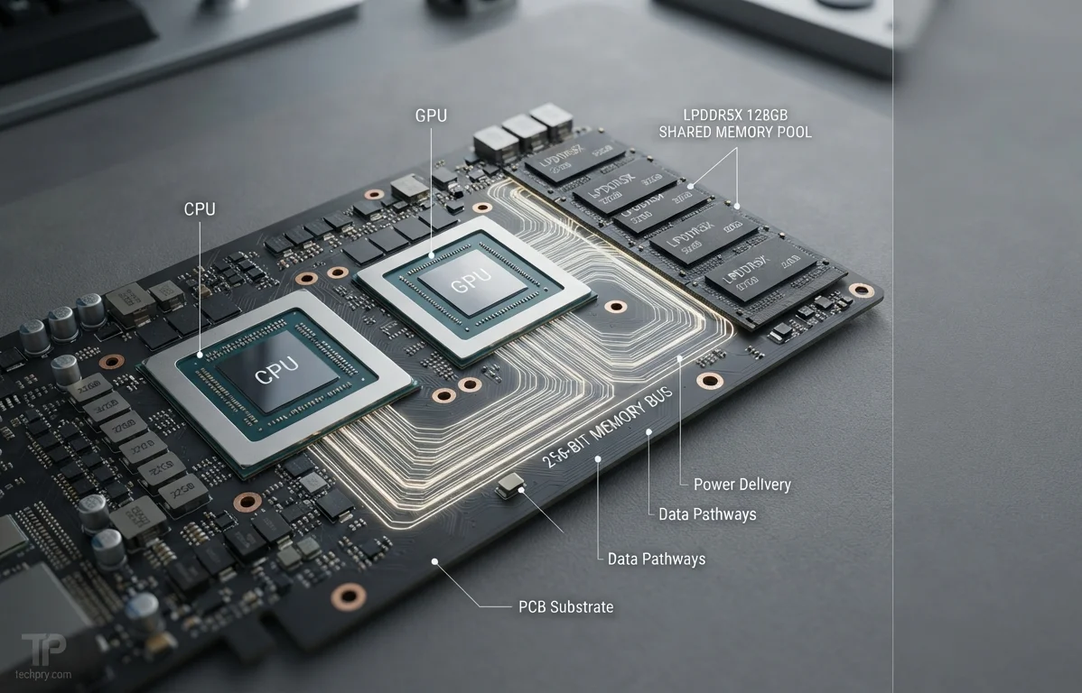
The GPU has no memory of its own. It uses shared with the CPU; NVIDIA's table lists up to 128 GB of on a 256-bit interface, and Technical City gives the same memory type and bus width. Technical City adds a 1067 MHz memory frequency and 273.2 Gb/s of bandwidth, and the spec states that the memory has no support.
In practice, capacity is a platform decision rather than a graphics-card one. The 128 GB figure is a ceiling, and every gigabyte the GPU uses is one the CPU cannot, so there is no fixed VRAM wall but no separate pool either.
The ECC line sits awkwardly beside the professional purpose in the spec: workloads that require error-correcting memory are not served here. Bandwidth and frequency come from Technical City alone, and the bandwidth unit is printed as Gb/s, so check both against the laptop maker's listing before relying on them for bandwidth-bound work.
Can the N1X (48SM) run large AI models locally?
Reportedly yes, though the claim is secondhand: shattered.io says NVIDIA and reviewers describe the shared memory design as letting the chip run large , reportedly up to 120-billion-parameter models, without the cloud. The same outlet lists up to 128 GB of unified memory shared between CPU and GPU, which is the capacity that claim leans on.
It is a reported claim, not a measured result, and it is about fit rather than speed: memory capacity decides whether a large model loads at all, while bandwidth and compute decide how quickly it answers, and the report says nothing about that second part.
The 20-core Grace pairing and what the N1X name means
Two names are in play, and they overlap. The spec says the GPU is used in the 20-core Nvidia N1X and recommends that CPU or above, while NVIDIA's table pairs the laptop version carrying the 6144-core GPU with a 20-core .
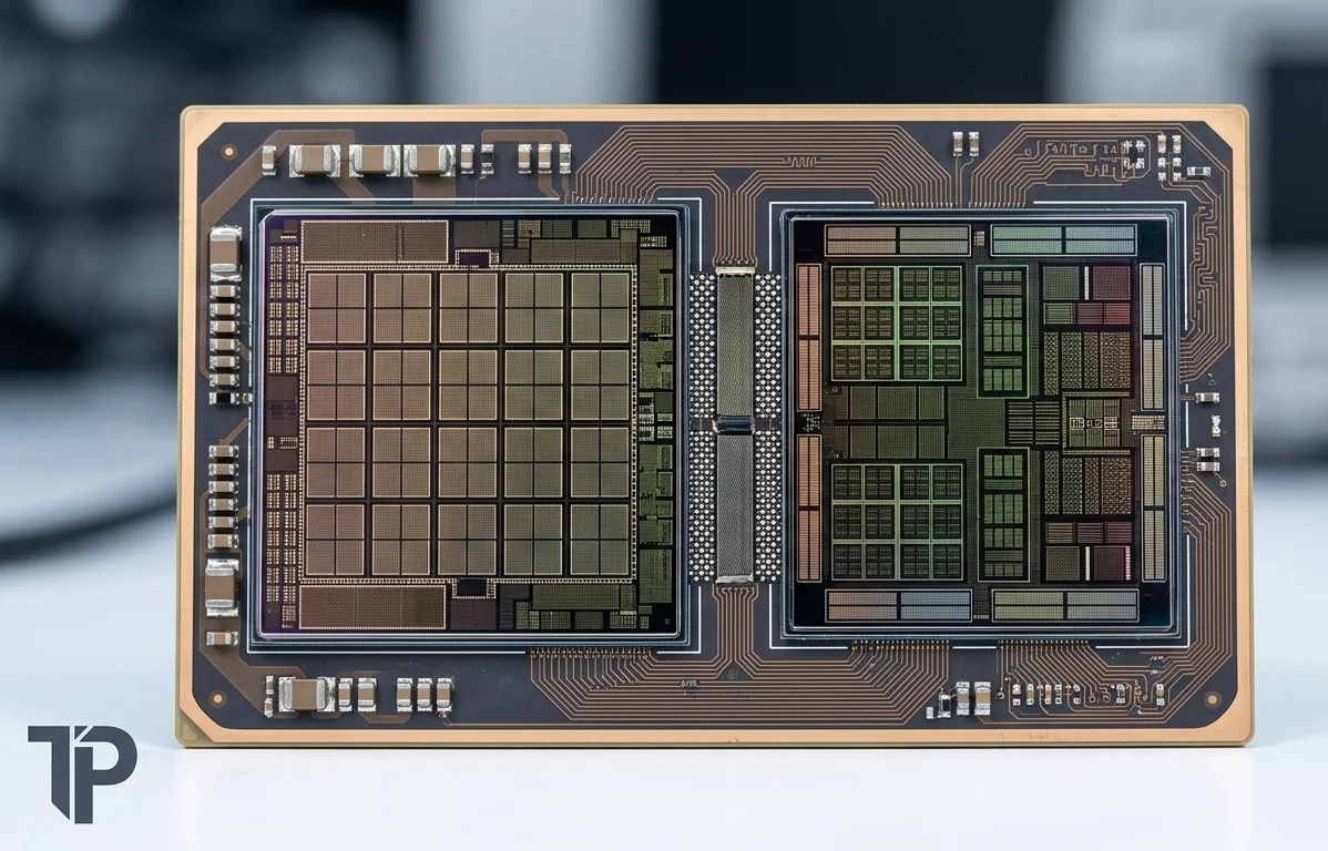
shattered.io reports that NVIDIA CEO Jensen Huang has also called RTX Spark by its internal name, N1X, so N1X on a spec page can refer to the whole platform as well as to this GPU configuration. The 48 in (48SM) matches the 48 compute units the spec lists. The same outlet says the CPU and GPU dies connect over at 600 GB/s.
The consequence is a fixed pairing. The spec's recommendation allows for tiers above the 20-core CPU, but the only CPU it lists the GPU in is the 20-core one, and a die-to-die link at that bandwidth is not something a buyer mixes and matches. Compare laptops by the platform, CPU included, not by the GPU line alone.
AI performance and power: 1 petaflop and a 45 to 80 W envelope
NVIDIA's table rates the laptop version with the 6144-core GPU at 1 petaflop of AI performance and a 45 to 80 W power envelope; shattered.io lists the same power range and specifies the AI figure as up to 1 petaflop of FP4.
The hardware behind it is 192 fifth-generation tensor cores, with named by shattered.io, plus an and NVIDIA AI Stack support in NVIDIA's table.
Read the petaflop figure as a low-precision peak. It is not comparable to the 31.2 TFLOPS of FP32 compute in the spec, which measures general shader math, and NVIDIA's table does not say which precision its 1 petaflop assumes. The FP4 label matters for the local-model claim above, because lower-precision formats let a larger model fit into the same shared memory, though that says nothing about speed.
The 45 to 80 W envelope covers the whole laptop chip, CPU included, and it is a range, so the point inside it that a laptop maker picks will shape sustained performance as much as any peak rating.
Supported graphics and compute APIs: versions at a glance
The spec lists 1.4, 3.0 and CUDA 12.1, and NVIDIA's table adds NVIDIA CUDA support, Microsoft , the Vulkan RT API and OpenGL 4.6.
| API | Listed version or support | Where it is listed |
|---|---|---|
| Vulkan | 1.4 | Spec |
| OpenCL | 3.0 | Spec and Technical City |
| CUDA | 12.1 (compute capability) | Spec, NVIDIA's table and Technical City |
| Microsoft DirectX | 12 Ultimate | NVIDIA's table |
| Vulkan RT API and OpenGL | OpenGL 4.6 | NVIDIA's table |
CUDA is the best-corroborated entry. Three lists give 12.1, and NVIDIA's table labels it CUDA capability, the hardware feature level rather than a toolkit release. OpenCL 3.0 is confirmed by Technical City as well. The remaining entries come from one list each, but none is disputed, which makes this the one block of the spec with nothing to second-guess.
DLSS support: DLSS 4 on the spec, DLSS 5 on NVIDIA's table
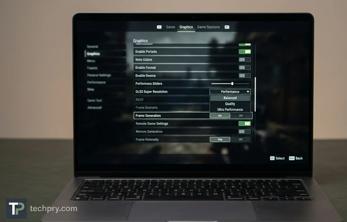
The spec lists DLSS 4 and Technical City marks DLSS as supported without naming a version, while NVIDIA's table for the laptop version lists DLSS 5. That same table marks these features as supported:
- DLSS Super Resolution
- DLSS Dynamic Multi Frame Generation
- DLSS 3D-Guided Neural Rendering
The evidence cannot settle which version label is current. NVIDIA's table is the maker's own statement for the laptop configuration, while DLSS 4 is the value attached to this GPU's spec listing, so anyone who needs a specific release for a specific game should confirm it on the exact laptop's own listing. For most buyers the feature list is the more useful half: it covers upscaling, frame generation and anti-aliasing, and Ray Reconstruction is the entry that ties directly to the 48 RT cores in ray-traced games.
Interface and connectors: PCI Express Gen 5, one HDMI output and no extra power connector
The interface is x16, and the spec, NVIDIA's table and Technical City all indicate PCIe Gen 5. Technical City alone adds support, a single HDMI video connector and no need for additional power connectors.
On an integrated laptop part these rows carry less weight than they would on a desktop card. The CPU and GPU dies are reported to link over NVLink-C2C at 600 GB/s, so the PCIe entry is probably a database convention more than the path CPU-to-GPU traffic takes, and the HDMI and power lines describe what a laptop maker will wire up rather than what the silicon dictates. Resizable BAR and the connector entries come from one list only, so confirm them on the specific laptop if they matter to your setup.
Manufacturing: a 3 nm node and 173.6 mm² die on the spec, 5 nm on Technical City
The spec says manufactures the GPU on a and gives a die size of 173.6 mm². Technical City lists a 5 nm process instead.
This is the one disagreement that cannot be checked by arithmetic. The fill-rate and FP32 gaps trace back to clock and TMU inputs, but nothing else in the figures depends on the node, so neither value can be tested against another number in the list. The die size appears only in the spec. If the node matters to your decision, prefer the maker's documentation for the specific laptop over either database entry.
Windows 11, Studio and Game Ready drivers, and NVIDIA software features
Everything here comes from NVIDIA's own table: it lists Windows 11 as the supported operating system, with both and Game Ready Drivers supported. The same table marks , NVIDIA G-SYNC, the NVIDIA App, and HDCP 2.3 as supported.
The driver pair mirrors the split personality in the spec, where the purpose is professional and the segment mid-range: Studio drivers for creative and professional applications, Game Ready drivers for games. Only Windows 11 is named, so buyers planning to run another operating system have no support statement to go on and should check before assuming.
Where it sits: a mid-range label, an Apple M5 Max comparison and no top-100 ranking
The spec puts the GPU in the mid-range segment and names the (40-core) as its Apple equivalent. Technical City ranks it outside the top 100 GPUs by popularity.
Neither entry is a performance measurement. The Apple pairing is the spec sheet's own mapping, and the popularity rank is Technical City's own ranking, which says little about speed. These are listed specifications, not benchmark results, so how a given laptop performs also depends on its cooling and on where the maker sets the power limit within the 45 to 80 W range.
Who the N1X (48SM) suits, and who should look elsewhere
The profile that fits is a Windows 11 laptop buyer who wants a large shared memory pool of up to 128 GB, local AI work with FP4 support and 1 petaflop of rated AI throughput, and a full DLSS feature set with both Studio and Game Ready drivers.
It fits less well if you need ECC memory, dedicated VRAM or a GPU you can replace on its own, since this is an integrated part sharing memory with the CPU. People running something other than Windows 11 should check, because NVIDIA's table lists only that. And anyone who needs firm clock, cache or FP32 numbers should wait for the figures for their specific laptop, given the seven values Technical City disputes.
Comments 0
Please log in or sign up to comment.